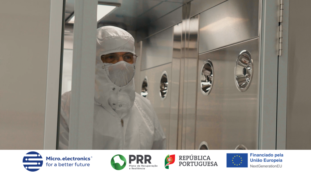


The second day of SEMICON Europa 2025 was marked by an intense agenda of networking, technical presentations and international recognition of the work carried out under the Microelectronics Agenda. Throughout the day, entrepreneurs, researchers and international entities visited the consortium’s stand, reinforcing collaboration opportunities and promoting the PPS actions already completed by the partners.
Among the highlights was the visit from the AICEP Berlin team, who emphasized the relevance of the Agenda for strengthening the country’s competitiveness and consolidating the national industry within the European microelectronics landscape.
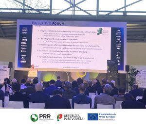
“Advanced Packaging” conference showcases new technologies and trends
One of the day’s main moments was the conference dedicated to “Advanced Packaging”, where international experts presented advances that are redefining the next generations of microelectronic systems. Topics covered included:
• Increased yield, reduced costs and improved reliability in advanced packaging processes;
• New processes such as laser dicing, copper fine-grain for hybrid bonding, and optimized underfill materials for thermal management in dense 3D structures;
• Sustainability practices, highlighting the use of more environmentally friendly liquids and chemical solutions;
• 3D integration and wafer bonding for automotive applications, where defect tolerance is minimal;
• “Zero-defect” 3D packaging concepts, with the potential to reduce costs up to 10× through more efficient workflows;
• Advances in high-precision metrology, including stitching-based visualization techniques with micrometer-per-pixel resolution.
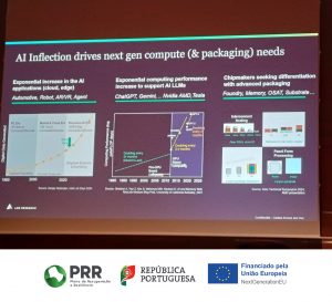
Another point of interest was the discussion on the impact of computational scaling for AI, analysing how interconnect topology and 3D integration contribute to overall system performance, positioning the package as an integral part of computational architecture.
Production focus: process innovation and factory automation
• Digital lithography for via patterning with ~2 µm resolution and high flexibility for small production volumes;
• Advances in inkjet printing for advanced semiconductor applications, achieving rates of around 1 second per wafer;
• The announcement of the first European low-volume FOWLP factory, inaugurated by AEMTEC;
• Fully automated systems for storing and handling high-value probe cards, essential in testing high-density wafers.
TechARENA: Sustainability and advanced materials in the spotlight
Several sessions also took place at the TechARENA, focusing on how sustainability is transforming the semiconductor industry — from facility design and manufacturing processes to the selection of greener advanced materials. Several experts presented practical solutions that reduce environmental impact while reinforcing Europe’s economic and industrial resilience.
The Microelectronics Agenda benefits from a total eligible budget of €67,572,099.37, of which €30,191,423.56 is financed by the NextGenerationEU initiative.
With project completion scheduled for 31 December 2025, Portugal aims to position itself as a leader in the global semiconductor sector, having already executed more than 80% of the budget and made significant progress in product development, sustainability and workforce training.