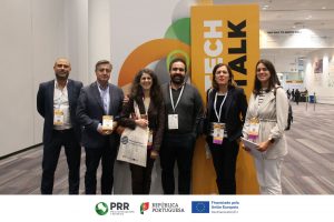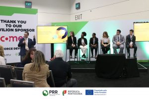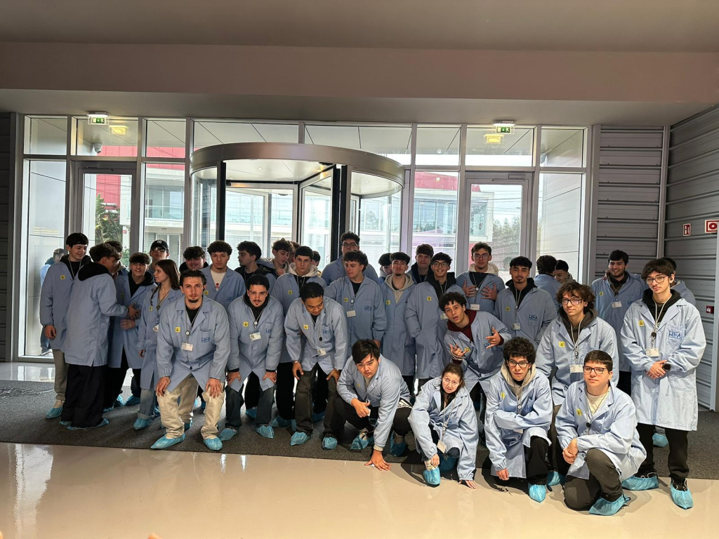


On the closing day of Semicon West, which is taking place in San Francisco (USA), the delegation made up of AIDA CCI, Inova-Ria and PCI – Creative Science Park – Aveiro Region, representing the Microelectronics Agenda, attended several sessions presenting important topics for the industry.
In the morning, Joel C. Warner’s session, from Samsung Austin Semiconductor, focused on humanoid robotics. The speaker offered his knowledge and perspective on the use of humanoid robots in the production process and in clean rooms, something in which large companies such as NVidia or, to take the example of the automotive sector, BMW, Mercedes, Hyundai and Tesla, among others, have been investing.
In this area, aspects under development stand out, such as the optimization of perception, locomotion and cognition, and the shapes of humanoid robots will be adapted to each specific need. The usefulness of this technology is obvious for more dangerous and error-prone tasks, so we can see a future in which humans will manage humanoid robots and, for more complex tasks, work in collaboration with this equipment. Boston Consulting Group Analysis estimates that the use of humanoid robots will grow in this industry by between 33% and 66%.
Also in the morning, there was a session led by Aske Bach Lassen on automation in factories with fully autonomous processes, namely autonomous systems for testing and assembling components. According to the perspective she shared, greater productivity will be achieved in dynamic production environments by investing in intelligent robots, adapted to the demands of the sector, such as Mobile Cobots.
At the end of the morning, Lisa-Marie Burns, Lorena Fregoso and Veronica Parks, respectively from the Fremont Unified School District, Stanford University and Ohlone College, shared their perspective on attracting talent, an area in which they are involved, highlighting the need to teach young students about advanced technologies, with the creation of programs that develop skills that will be attractive for the future integration of graduates into companies.
There was also time in the morning to attend a session by John Howarter, from Purdue University. He presented the university’s ongoing programs to attract students to the semiconductor industry, from the involvement of high schools to the development of Summer Training programs, certified and paid for by companies, in which young people are encouraged to participate with a view to greater employability. It was also possible to hear testimonies from students who are specializing in chip design and the manufacture of more sustainable materials in semiconductors.
In the afternoon, the session by Beth Unger and Sajan Saini, both from MIT, focused on the development of sustainable chips and how to raise awareness of sustainability in this area. From their perspective, the goal can be achieved by creating workshops, university courses, bootcamps, internships, online training and, finally, enlisting the support of industry leaders who can influence attention to the issue, in a synergy between companies, academia and political power.
In the block of sessions “Driving the next generation of devices with advanced lithography, heterogeneous integration and packaging”, the presentation by Bryce Chi from ONTO Innovation in Taiwan addressed the challenge of manually inspecting defects in silicon wafers, proposing as a solution mixed artificial intelligence processes with Deep Learning Neural Networks.
In traditional semiconductor packaging, manually reviewing defects after automated optical inspection (AOI) is an arduous task for technicians. It is difficult to avoid human error when reviewing thousands of defect images every day.
Automatic defect classification (ADC), integrated into AOI mechanisms, can reduce the number of defect images that need to be reviewed by technicians. The resulting software application developed by ONTO Innovation uses CNN (Convolutional Neural Networks) algorithms, a technique used for image recognition, DNN (Deep Neural Networks) and KNN (K-Nearest Neighbors), used for image recognition. The results obtained are very satisfactory and make it possible to combine the benefits of the different algorithms, ensuring a more reliable and accurate classification of defects.
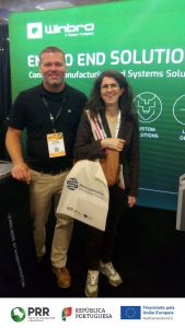
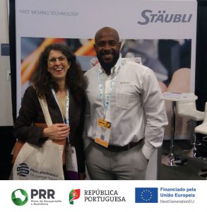
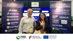
In terms of prospecting, there were meetings with Opentext, a company that focuses on data protection and cybersecurity, also applied in the semiconductor industry; with Stäubli, which provides technological solutions in the areas of electrical and fluid connectors, textiles and robotics; Robovision, which introduced us to a platform that, using artificial intelligence, can be used for quality control/defect detection in various sectors: electronics, agriculture and health; Winbro, which provides innovative cutting-edge laser and EDM technologies that promote renewable energies.
We ended Semicon West with an insight into updates on needs, trends, new technologies, materials, processes and specialization programs in the North American microelectronics industry sector. Opportunities were also created for present and future synergies with American, Korean, Spanish, British and German companies, among others.
The semiconductor ecosystem must increasingly focus on key pillars and create more efficient forms of supply and cooperation within the value chain. The focus must be on training talent, innovation, photonics, automation, creating strategic synergies, sustainability, energy, advanced lithography, using more efficient materials and processes, reducing waste, reusing components, the role of artificial intelligence and quantum computing. These key areas of action can significantly boost the development and growth of this sector.
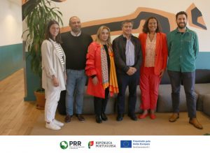
The delegation also met at the end of the day with the AICEP Delegation in San Francisco to discuss the Agenda’s developments in the sector and foresee current and future cooperation opportunities.
The Microelectronics Agenda was created as part of the mobilizing agendas of the Portuguese Recovery and Resilience Plan with the aim of strengthening the production and innovation capacity of the national semiconductor and microelectronics industry. It involves a group of 17 partners and seeks to help position Portugal at the forefront of the semiconductor management, production, distribution and recycling market, capable of supplying Europe and other countries worldwide.
The 25 new products, processes and services resulting from the Agenda aim to transform the microelectronics sector and contribute to its resilience, competitiveness and ecological sustainability, and will enable the Portuguese ecosystem to monitor and anticipate the sector’s needs.
The “Microelectronics Agenda” project runs from January 1, 2022 to December 31, 2024 and is co-financed on a non-repayable basis for a total eligible amount of €67,493,749.13 by the Portuguese Recovery and Resilience Plan through NextGenerationEU.