

As part of its activities in the Microelectronics Agenda, INL – International Iberian Nanotechnology Laboratory, has developed a brochure showing its developments and services in the Microelectronics and Semiconductors sector, which can be consulted at this link: https://bit.ly/3UyWa3N
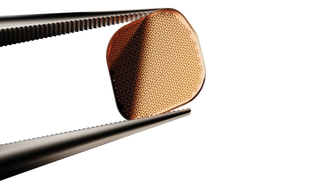
This partner provides services in its micro and nano manufacturing infrastructure (INL MNF Facility) from the early stage of the design conception till the last phase. It unfolds from the process integration and development to the most expert process engineers on the latest core technologies. The INL MNF Facility is prepared for small pre-productions series, facilitating technology transfer to industry and their standardization also in multi-project wafers (MPW). Its flexibility, focus, and yield-oriented approach enable quality assurance and ultimately the development of robust proof of concepts.
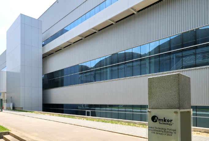
As part of their activity, they are developing methodologies and materials to boost advances in wafer-level packaging technology and MEMS&Sensors, in particular increasing the density of interconnections to meet the current needs for miniaturisation and performance in the sector. These developments will be achieved through close collaboration between INL, which is responsible for part of the R&D effort, and ATEP, which is responsible for the subsequent integration of technologies, materials and processes into its operation.
Find out more about INL and its activities here.